Scanning electron microscopy (SEM) or SEM analysis is a powerful analytical technique to perform analysis on a wide range of materials, at high magnifications, and to produce high resolution images. TWI’s extensively equipped electron microscopy suite allows many different types of sample to be analysed, giving resolution greatly exceeding that of conventional light microscopy.
SEM Imaging
SEM relies on the detection of high energy electrons emitted from the surface of a sample after being exposed to a highly focused beam of electrons from an electron gun. This beam of electrons is focussed to a small spot on the sample surface, using the SEM objective lens. Variables like the accelerating voltage used, size of aperture employed and the distance between the sample and electron gun (working distance) can be optimised to achieve the best quality images.
There are two modes of electron detection which allows for different types of imaging and analysis, each giving vital insights. Backscattered electrons can be detected to give contrast based on different chemical compositions across an image. Secondary electrons, emitted close to the surface of the sample, give information about the surface topography.
Energy-Dispersive X-Ray Spectroscopy
Each of our SEMs are equipped with energy-dispersive X-ray (EDX, also referred to as EDS) spectroscopy facilities. When exposed to the electron beam, an atom emits characteristic X-rays unique to its atomic number; this allows a sample’s elemental composition to be analysed, whether at a single point or over a large region, including line scanning and elemental mapping. Semi-quantitative analysis can also be performed to assess the chemical composition of a sample. TWI also has capabilities for wavelength-dispersive X-ray (WDX) analysis to detect light elements, such as oxygen, nitrogen etc. Combined with conventional SEM analysis, EDX can give a fuller insight into the local composition of a sample.
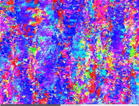
Electron Back-Scattered Diffraction
One of the most powerful quantitative techniques is electron back-scattered diffraction (EBSD), which produces microstructural maps, presenting high-resolution crystallographic data and analysis of phase distribution, misorientation (strain), grain size and distribution, and preferred crystallographic orientation (texture). Once a highly specialised technique, this can now be performed routinely. The technique is highly dependent on excellent sample preparation, which can be arranged through our metallography laboratories.
TWI’s Electron Microscopy Suite
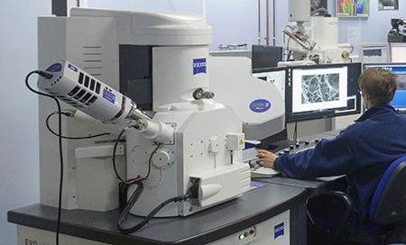
This high-performance LaB6 environmental scanning electron microscope (SEM), fitted with EDX and WDX detectors, allows for imaging alongside SEM chemical analysis of a wide range of specimens. It is also equipped with a large sample chamber to accommodate many different sample dimensions.
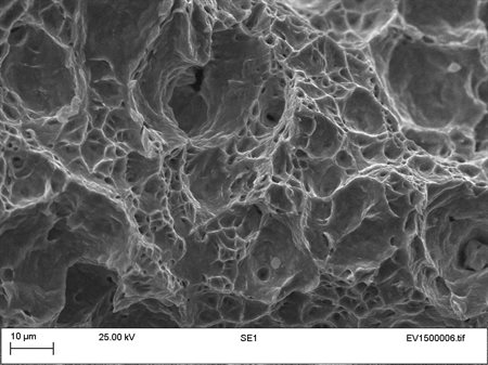
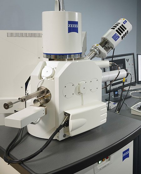
This scanning electron microscope allows very high-resolution imaging, with clear SEM images and electron microscopy analysis beyond 50,000× magnification, allowing analysis from micron to nanometre scale. This can be an essential tool for characterisation of test samples, failure analysis, fractography in materials including metals, polymers and ceramics, and analysis of deposits, contaminants and powders. Equipped with EBSD facilities, simultaneous EBSD and EDX data acquisition can be performed.
Knowledge and Capabilities
With close links to industries in many sectors and a wealth of knowledge and experience, TWI offer a range of high quality scanning electron microscopy (SEM) analysis and imaging services. This ranges from small-scale rapid-response material characterisation from one of our experienced experts to combination as part of a larger project for compliance testing or failure analysis.
This ranges from small-scale rapid-response material characterisation from one of our experienced experts to characterisation work as part of a larger project for compliance testing or failure analysis.
For more information visit our microscopy page or email contactus@twi.co.uk.