Thu, 20 August, 2020
TWI has been working on the collaborative CITCOM Project, which is now set to be highlighted on the European Commission's Innovation Radar platform. The project saw the development of a purpose-built X-ray system for the inspection of small electronics known as MEMS devices. CITCOM involves 12 European industrial partners and RTOs coordinated by CSEM SA.
These MEMS devices, which are typically composed of materials such as silicon, are continuously getting smaller as the manufacturing techniques keep improving, this in turn requires the inspection method to continue to improve to cope with the increasing challenges of the miniaturisation of MEMs devices. To meet the increasing demands of high end MEMs manufacture and inspection, the CITCOM project was put together via EC funding. The project was created to develop an inspection method that could assess the highly 3-dimensional MEMs devices. Two systems were developed during the project, a plenoptic camera system and an X-ray system. With these two systems the MEMs manufacturers would be able to assess the full volume of the MEMs samples, including both external and internal parts. High resolution was a necessity for the project to capture the miniature defects that occur in these samples. As part of the project, TWI and the consortium have been able to build and integrate an X-ray system capable of 0.5um spatial resolution.
 Harry Atherton
TWI’s Non-Destructive Testing Senior Project Leader, Harry Atherton revealed how TWI helped achieve this, as well as explaining some of the challenges that were involved:
Can you explain the industrial need for developing the CITCOM system?
MEMs and micro-manufacturing has developed drastically over the past 20 years and, with the large influx of production, research has to be undertaken to improve the manufacturing process. MEMs are being integrated into more and more technologies. As the manufacturing technologies have improved, the MEMs have been getting smaller and more 3-dimensional in structure. The 3-dimensional nature of MEMs samples means that the standard integrated circuits (IC) (highly planar in design) inspection tools are not sufficient to assess the volumetric design of the MEMs samples. Volumetric inspection is critical for MEMs manufacture as it can allow the user to have far greater confidence and yield in their product. CITCOM has been created to address the continuous industrial needs of MEMS and micro-manufacturing, which will offer a near-line production inspection and measurement system for micro-components. The final system will be developed and demonstrated at TRL7.
What were the main challenges of the project?
The main challenges for the CITCOM X-ray system was the selection and design of the major components - the X-ray source, X-ray detector, X-ray manipulator, the table and the shielding and safety system. Selecting and refining the major components to yield the best performance whilst also managing the financial aspects of the design. The ability to achieve high quality, sub-micron resolution images was the necessary outcome for the project. This aim entailed some challenges with regards to low attenuation from MEMs materials, large areas for wafer inspection (up to 8” wafers), near line inspection (short inspection time) and price. The CITCOM system had to be designed with the future mind-set of taking the system to market, as it was in the higher TRL brackets (TRL 7). Each major component has its individual challenges and these needed to be integrated together in the final assembly, the relationship between each and every component was critical to ensure that our final objectives were achieved.
What were the stages required for the completion of the project, and what did they involve?
There were four major stages for CITCOM project; research, design, assembly and integration. The research at the start of the project was the foundation that the project was to be built on. This stage also included the necessary requirements of the system, which were put together as a consortium with great input from MEMs manufacturers, Phillips, VTT and Microchip. The system requirements then directed the research into selecting the correct major components for the system. Papers, journals, professionals, suppliers and field trials were used to assess which components would be best suited for the CITCOM application. Once the components were finalised through a rigorous selection process, the design of the system was required. A design that encompassed all the major components in one standalone system. The assembly of the X-ray system was over a long period of time and had its phases, with initial testing on the system conducted in a radiation bay. This initial testing included mounting the major components in place, testing functionality and fine tuning positions. Eventually the system was fully assembled as a standalone system in a self-contained cabinet to shield operators from the ionising radiation from the X-ray source. Once the assembly was completed, the integration phase began. This involved developing the overall control system for the unit to allow harmonious and synchronous communication between all the components as well as the development of an easy to use interface for the operator to use seamlessly.
How does the system work?
X-rays are emitted from the X-ray source, the X-rays then come into contact with the MEMs wafer. Depending on the geometry and material of the MEMs wafer, some X-rays will be absorbed by the sample and some will pass through (this is also dependant on the energy of the X-ray voltage). Much like a camera, the image captured on the X-ray detector depends on what areas were exposed to X-rays. This is the fundamental setup for radiographic inspection.
The CITCOM system has been setup for the inspection of MEMs wafers up to 8” diameter. The inspection data gathered during inspection can be related directly to the wafer map. The operator can set up the inspection recipe to their choice, using high magnification for high resolution images or lower magnification for shorter scan times. The operator can choose whether to inspect the full wafer, all the good dies, individual dies or areas of each of the dies. The operator has full control over a wide range of inspection recipes, all of which can be tailored to achieve the best results for their wafer inspection.
What were the final outcomes of the project and how did TWI help deliver them?
During the CITCOM project the consortium has come together to develop a global system that can volumetrically inspect MEMs devices. This system consists of two individual systems which complement each other; a 3D vision system and an X-ray system. Both systems are capable of holding and inspecting up to 8” wafers in size. These systems are now complete and are ready for installation within a MEMs manufacturing facility for near-line evaluation.
The 3D vision system consists of a micro-electrical wafer prober with a plenoptic camera. The camera has the ability to create high resolution 3D depth maps of the MEMs samples under inspection. The 3D vision system gathers volumetric information of the sample under inspection, which gives the operator the ability to assess the 3D metrology of the sample and detect defects on the sample surface.
The X-ray system gives the CITCOM global system the capacity to assess the internal volume and structure of the MEMs devices. The penetrating power of X-rays means that the internal volume can be assessed non-destructively and capture information that the 3D vision system cannot obtain. TWI has been responsible for the development and integration of the CITCOM X-ray system, this included the specification and selection of the major components within the X-ray system. The X-ray source used is the Nanotube 60kV N2 by Excillum AB (one of the consortium members), and the source was enhanced during the project to further fit the use for the purpose of MEMs inspection.
All the major components were designed and assembled at TWI, Cambridge. The system was fully integrated and tested on site. Special attention was paid to the shielding and safety system designed by Electron-X, which means that the CITCOM X-ray system is a fully contained/shielded X-ray system that adheres to IRR19. The control software and graphical user interface (GUI) has been designed and developed by TWI to ensure that the operator has the capability to conduct a wide range of radiographic inspections of the MEMs samples. Ease of operation was key for the development of the user interface.
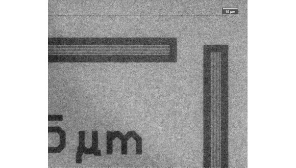
The X-ray system has been able to achieve a spatial resolution of 0.5 µm, enabling detection of sub-micron defects within the inspected samples. See image below.
Both the 3D vision system and the X-ray system are now ready for deployment at a MEMs manufacturing site to further assess their use and functionality for the manufacturing line.
The CITCOM project has received funding from the European Union’s Horizon 2020 research and innovation programme under grant agreement No. 768883.