Mon, 21 December, 2020
The collaborative project CITCOM, short for ‘A Complimentary Inspection Technique based on Computer Tomography and Plenoptic Camera for MEMS Components,’ has had a successful final project review with an EC project offer on 15 December. TWI has been involved in CITCOM and leading the development work of a nano-focused X-Ray machine for scanning MEMS wafers of up to 8 inches.
TWI has teamed up with project partners Excillum and InnotecUK on the development of a nano-focused X-ray machine. The CITCOM X-ray system has been designed and assembled with the purpose of inspecting up to 8” MEMs wafers. The X-ray system consists of three major components, the X-ray source by Excillum, the X-ray manipulator by InnotecUK and the X-ray detector. Refined selection and product development of these three components have allowed the CITCOM X-ray system to be able to achieve 0.5 µm spatial resolution. The proven high-resolution CITCOM X-ray system allows MEMS manufacturers the possibility to detect sub-micron defects within wafers and improve the reliability and yield of the wafer manufacture. The X-ray source for the CITCOM system is the Nanotube 60 kV N2 from Excillum, which offers a high maximum resolution of 150 nm, high voltage of 20 – 60kV and target power up to 2.5W. The X-ray manipulator was designed by InnotecUK and can manoeuvre up to an 8” wafer in horizontal movement, as well as vertical movement and allows full 360° rotation. The X-ray detector is a large 5.5MP charge integrating detector with a fine pixel pitch.
The CITCOM project aims at developing an in-line MEMS inspection system including a fast plenoptic scanning and a standalone X-ray system that is capable of operating detailed X-ray scan in any near line MEMs manufacturing laboratory. The CITCOM X-ray system is operated via control software with a TWI developed graphical user interface (GUI) for easy user interaction and operation for wafer inspection. The users are able to freely manoeuvre the samples to the point of interest, align the wafer sample to known wafer map, zoom in more than 400x geometrically while still retaining high image contrast, and select before four automatic scanning functions including full area scan, single die scan, all good die scan and area scan of all good dies.
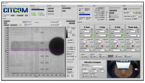 Figure 1. CITCOM X-ray system GUI
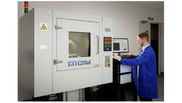 Figure 2. CITCOM X-ray system
The CITCOM X-ray system has been integrated and validated at TWI. Extensive system validation work has been conducted and achieved a successful outcome. The system has been demonstrated to end users for its capabilities of detecting various MEMS solder related defect types such as missing, spotted and irregular sized solder. The system has also demonstrated high repeatability, where less than 3% deviations were observed between two separate scans at the same locations on the wafer sample. TWI is looking forward to strengthening the collaborations with end users in 2021 for the system trial on-site.
The CITCOM project has received funding from the European Union’s Horizon 2020 programme under grant agreement No 768883.