TWI
Neil Tomlinson
Machine Vision Products
Paper presented at BINDT 2006 Conference, 12-14 September 2006, Stratford-upon-Avon, UK.
www.microscan.eu.com
Abstract
Automated Optical Inspection (AOI) for non destructive detection of defects in Printed Circuit Boards (PCBs) is an established technique for quality control in the production line. The reliability of detection of defects is influenced by a number of factors including, the resolution of the camera, the repeatability of placement of PCB with respect to the camera, and the threshold values used in the defect algorithms for deciding if a board passes orfails. This presentation details the development of an in-line system employing a computer controlled high resolution camera and PCB transit system. A golden image of a 'good' PCB can be obtained, and subsequently an active image of aPCB being inspected can be subtracted from it. Any resulting difference can be used to pin point potential defects and used for automatic defect recognition. Ideally for good reliability of defect detection the reference positions of the reference and target images should be identical. Intensity based image registration has been developed to compensate for the inevitable misalignment resulting from mechanical placement differences. To further identify defects, a variety of pixel based image processing and feature classification algorithms are deployed.
1. Introduction
The smaller components and higher component densities on today's PCBs have driven manufacturers to demand automated inspection systems on their production lines. Traditionally In-Circuit Testing (ICT) and functional testing is used to diagnose faults after assembly of PCBs. However, it is more cost effective to test for defects and make a repair at an earlier stage in the manufacturing process. Additionally, because of the ever increasing component and circuit electrical density, the electrical node access that is required for ICT can be limited and electrical test coverage decreased.
TWI has been working with partners on a European cooperative project seeking to develop an in-line PCB inspection system employing different techniques to provide full coverage of all PCB defects. Modular inspection systems are being developed, where acoustic examination, thermography and X-rays are to be used in conjunction with AOI to test for defects on areas of interest on a PCB. The objective of this paper is to present the development thus far for the AOI module, just one of the four techniques that will be integrated to form the final combined system. The work for the AOI part has proceeded in two phases:- phase one which is detailed in this paper involved the construction of basic AOI hardware together with the development of a software application to provide the frame work for testing algorithms in the AOI experiments. In addition a conveyor was constructed and control of it within the software framework was implemented. Phase two which is still ongoing at the time of writing, is the further improvement of the techniques developed in phase one, together with trials in a factory environment and integration with the other inspection techniques.
2. Typical defects found in PCBs
Assembled PCBs can suffer from many defects and it is highly beneficial for these defects to be detected early on in the production stage, as the later the failure is detected in the PCB assembly line the more the rework/repair cost.
A modern PCB assembly line comprises at least three key stages: solder paste printing, component placement and reflow oven. In solder paste printing a stencil is placed in contact with the board and a wiper blade passes over the stencil thereby depositing the paste through the stencil holes. Optically inspecting the board immediately after this stage can highlight if the stencil has misaligned with the board, and if sufficient paste as been deposited. The nextstage is component placement where the PCB is populated with the insertion of components. Immediately inspecting after this stage verify's the operation and accuracy of the pick and place machines. Typical defects that can be detected are missing, offset skewed and flipped components, and wrongly placed components. Once the solder paste has been deposited and the components placed, the last stage is the reflow oven. Reflow cooks the PCB and solders all of the pads simultaneously. Optically inspecting after reflow enables verification of solder joint quality, evidence of excess and insufficient solder, and component migration. Other defects include the phenomenon called tomb stoning in which a component positions itself erect at one end as result in difference in surface tension of both ends during solder melting or solidification. Another related defect is the lifted lead, where the lead is not in good contact with the solder. Bridging and shorts can also be easily visualised after reflow. Many of these defects are contributed to from a poor solder paste printing process but only prevail themselves after reflow. Figure 1 shows examples of some of thePCB defects that have been mentioned and which are visible after reflow. Some good components are also shown for reference.
For the solder paste printing and component placement stages, the role of AOI is in the defect prevention category, as rework can remove the cause of defects. After the reflow stage inspections cannot prevent future defects and AOIfalls into the detection category.
Since AOI works by comparing an acquired sample image to a defect free 'gold standard' sample image, any causes of defects in the sample image can be inherently detected due to cosmetic differences. Therefore the same AOI technique lends itself to post testing to any of the three stages.
Fig. 1. PCB Component defects a) Good positioned Ceramic Capacitor; b) Tilted Ceramic Capacitor; c) Missing Ceramic Capacitor; d) Lifted lead on Dual In Line (DIL) Integrated Circuit (IC); e) Unsoldered lead on Thin Quad Flat Pack (TQFP) IC; f) Good positioned resistor but flipped; g) Tomb stoned resistor - open solder at one end; h) Solder Bridge/short on DIL IC
3. AOI prototype development
3.1 Specification
A Hitachi KP-F120 CCD camera with 1392 x 1040 effective pixels is used together with a 1:1.4/16mm lens. Typically the height of the camera is positioned at 27 cm above the PCB giving a field of view of approximately 120 x 120 mm.The distance was established empirically and depended on the type of components under inspection. In order for the algorithms to function reliably an area of at least 20 x 20 pixels is required to represent the component area under inspection. If for example a component having very fine pitch leg spacing was under investigation then the camera would have to be positioned closer to the component in order for the AOI system to reliably detect any defects then say compared to checking for missing resistor components. Images are acquired from the camera by a Nexeon - PCI CameraLink, 80MHz pixel clock single input frame grabber with 32MB frame buffer mounted in a personal computer (PC). A Software framework has been developed to allow images to be acquired and processed and different algorithms tested. Figure 2 shows the current experimental set up. In phase one of the project only ambient lighting is used to illuminate the PCBduring the inspections and lighting conditions were therefore not optimised. In phase two, the intention is to mount a white LED ring light on the camera objective to give a uniform and shadow free illumination of the PCB, and to enclose the inspection area in light proof panelling.
3.2 System Integration
An edge belt conveyor has been developed to enable the system to be placed in-line with existing in-line transfer systems. Using edge belts and side rails ensures minimum movement of the PCB transverse to the conveyor motion, and through a mechanically adjustable back rail allows for different sized PCBs.
An opto sensor mounted on the conveyor and comprises an infrared light emitting element and an infrared light receiving element that is used to detect when the front edge of the PCB is in the vicinity of the opto sensor. Upon detection of a PCB, control logic in the conveyor automatically stops the conveyor and a bPCB_PRESENT logic signal is toggled. The conveyor belt drive motor includes a break that guarantees mechanical stop placement of the PCB to within 0.2 mm. To advance the conveyor again the conveyor control logic must receive a bADVANCE signal and this signal is sent from the control PC.
PCB equipment suppliers use a standard called SMEMA [1] to facilitate the interface of their equipment at a mechanical and electrical level. This standard has been implemented for the prototype and includes standardisation of conveyor height, PCB edge clearance, and in-line system to system electrical communication. As such the AOI system behaves as a pure 'pull' type system, where the PCB is not released or moved to the next process step until authorised or pulled by a vacancy downstream. [2] The bMACHINE_BUSY and bBOARD_AVAILABLE in/out provide for the system to system communication. All the signals are communicated to and from the PC via an off-the-shelf USB controlled module providing computer controlled input and output control signals. [3] The advantage of using the SMEMA standard is that a separate cell controller is not needed to manage the flow of the material. Figure 3 shows two inspection systems, a machine (n) and a machine (n+1) both comprising a control PC and conveyor together with the signals for interfacing with the conveyor and the signals for communication between the systems.
4. Automated defect detection
Image subtraction is commonly used to highlight differences between two relevant images. [4] It was adopted in the software framework, together with other digital image processing techniques, for the identification of missing components in PCBs in a production environment. The main procedures include: image acquisition and pre-processing, image subtraction, residual image analysis and characterization, defect interpretation and recognition, and the sentencing of the PCB being inspected. Figure 4 shows the flowchart representing the sequence of steps for the AOI operation.
4.1 Image acquisition and pre-processing
Prior to conducting real PCB inspection, a golden image is captured and stored in a computer which serves as a reference. In this golden image, all components exist on the PCB with sufficient precision according to manufacturing specifications. Subsequently, live images of a PCB being inspected in a production line are taken and subtracted from the golden image. The resultant residual image reveals any differences between the target PCB image and the reference image. Where there are bright pixels remaining, a component is likely to be missing. This can be done automatically by a whole image field intensity check, thus achieving an automated inspection of missing components.
Due to the limited field of view of the imaging system with a sufficient image resolution, it is always necessary to take several local images of a PCB. These local images are then stitched together to form a complete image. With aproper mechanical positioning system, this can be implemented automatically. The only potential problem is misalignment between different local images as shown in Figure 5 because of limited precision of the mechanical positioning system. This will greatly affect the reliability of the algorithms, usually resulting in an increased false alarm rate. To correct for these, rigid image registration [5] is needed during the stitching process. PCB manufacturers normally put fiducial marks in the printed circuit artwork to provide common measurements for all steps in the assembly process. Fiducial marks are often put locally to particular components that require more precise location. These fiducial marks can be used to guide the placement of corresponding local image to the correct position. For each image the user is required to indicate to the registration algorithm where the fiducial mark is. Ideally, at least two fiducial marks should be available in each local image to facilitate registration. If no official fiducial mark is available then another constant positioned mark can be used such as an electrical test point.
4.2 Image subtraction
Given two images, one golden image and a live image, it is digitally convenient to perform an image subtraction. To enable the subtracted image to be visualised appropriately, intensity scale adjustment is performed. This is to project the subtracted intensities to a dynamic range available for the computer display, either by linear projection, step-size projection, or non-linear projection.
It is apparent that, to ensure a successful image subtraction that reveals only those differences corresponding to missing components in a target PCB, all the imaging parameters must be kept constant, both for the golden image andfor the live images of PCBs in a production line. For those PCBs that have some highly reflective surfaces, a slight change in illumination will cause considerable variation in the intensities of the captured image. As a result, significant residual intensities remain after image subtraction. This is one of the main sources of false alarming in the PCB inspection. Figure 6 shows the results of one typical PCB inspection. Most of the residual bright intensities are associated with real defects, i.e. missing components, while some stem from the shinning variations. They need to be further characterized based on context analysis in the next step.
It should be noted that, the locations of components in a PCB may not keep identical across the whole series of PCBs being inspect even if the fiducial marks are exactly stable in position. This is another cause of excessive residual bright pixels. To overcome this problem, local image registration can be applied to correct for local misalignment of separate components. An extra benefit of this approach is the extension of the detection capability to include the identification of orientation sensitive defects. For example, an upside down capacitor can be identified when a 180-degree local registration is conducted.
4.3 Residual image analysis and defect identification
The residual intensities are analysed by taking account of the context of original images. Firstly, a threshold operation is performed to highlight the residual pixels with high intensities. The optimal threshold is found from the histogram of the original image. Those pixels with high intensities are characterised as object pixels while others are characterised as background pixels. A grouping operation is followed to merge together separated pixels belonging to a common component:- operations of medium filtering, corrosion, and void filling are applied so that isolated bright residual pixels can be eliminated and only those bright spots corresponding to real missing components are retained. Subsequently, potential defects are identified when there are a group of bright pixels and in addition where their original image does not exhibit near-saturated intensities. Near-saturated intensities are mostly likely corresponding to surface shining.
|
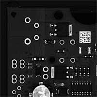
a) Golden image
|
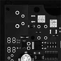
b) Target image
|
|
|
|
|
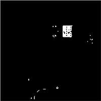
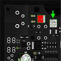
c) is the final residual image by subtracting (b) from (a). This leads to the identification of potential defects indicted in (d) by green boxes overlaying on the original target image
|
d) Big arrow in (d) indicates a false alarm due to shinning of the soldering surface, this is high lighted for illustration purposes only
|
|
|
|
|
Fig.2. AOI results for application of defect detection algorithms [Nicholson, Gao et al., 2006]
|
5. Results and discussion
A framework for testing AOI algorithms has been established. The system developed in phase one allows region of interests (ROIs) to be easily set up via the graphical user interface. In principle, generic types of detect can bedetected based on a comprehensive comparison of ROIs in the reference image and target image. However, as there are a variety of parameters affecting the quality of optical images taken in a dynamic production environment, preliminary test results showed that considerable false alarms would occur if the predefined threshold level for certain ROIs were not optimal. Optimising the configuration including the threshold level usually requires an iterative process, involving a series of trials with different bad boards and can be time consuming. The current direction is to develop a separate and more automated approach focusing on detecting a specific type of defect, missing component, rather than aiming at the whole spectrum of defects.
In this specific approach, the user marks a couple of reference points based on the location of fiducial points on the PCB. Subsequently, whole images (comprising several smaller images) of PCBs in a production line are taken, and the software will automatically detect missing components. In view of minor misalignments of local images of a PCB due to inevitable mechanical positioning errors, rigid body image registration is applied. This reduces the phantom residual bright pixels and thus improves the reliability of the whole system. For those false alarms caused by ultra-sensitive intensity variations in shining surfaces, context analysis is performed so that those bright pixels most likely exaggerated by the shining effect are ignored to keep false alarms to a minimum. Preliminary test trials have been promising, demonstrating the robustness of this approach.
For generic types of defect in PCB, the current AOI system is still being optimized in terms of predefined configurations for a specific series of PCB. One of the major challenges is to find a proper measure to correct for excessive intensity variations due to shining effects when slight ambient illumination change occurs. As an initial approach, intensity based similarity analysis of each ROI will be complemented with context and shape analysis to reduce the false alarming rate. Other computational techniques such as factor analysis and principal component analysis might be employed as well.
In theory it is possible to detect changes in the shading of imaged solder joints and therefore the quality of the solder joint itself. However, because only an ambient light source was used in phase one of the project, it was not possible to get reliable pass and fail indications.
6. Conclusions
A basic AOI system has been developed that is suited for defect inspection after the component placement or reflow oven stage in the PCB assembly line. In particular, results have shown that the developed prototype is highly suited to detecting missing components.
An obvious disadvantage of AOI is that it cannot be utilised when there is no visual coverage. Ball grid arrays, shielding, covers, fine pitch are all inhibitors to the application of AOI. The final goal of the project is to developa system comprising a combination of different Non Destructive Techniques (NDT) techniques to provide full coverage of all PCB defects.
The adoption of the SMEMA standard not only enables the easy integration of the prototype with PCB assembly systems in a factory environment but also permits integration with other NDT techniques that are concurrently being developed in the project.
Future work will include enhancement of the algorithms, the provision of a uniform light source in the prototype, and a computer controlled motorisation for panning the camera over the PCB.
Acknowledgements
The results from this work are part of the CRAFT programme: Development of comprehensive in-line quality control system for printed circuit board assemblies, Acronym MICROSCAN, COOP-CT-2003-508613. MICROSCAN is a collaboration between the following organisations: TWI Ltd, X-TEK Systems Ltd, Lot Oriel GmbH, Machine Vision Products Inc, Microtel Technologie Elettroniche SpA, Beta Electronics Ltd, Ultrasonic Sciences Ltd, Goodrich Control Systems Ltd,Fraunhofer-Gesellschaft zur Foerderung der Angewandten Forschung E.V. and Kaunus University of Technology. The project is co-ordinated and managed by TWI Ltd and is partly funded by the EC.
References
- SMEMA Interface Standard 1.2, Surface Mount Equipment Manufacturers Association
- Burda, Richard, 'Controlling Material Flow and WIP on Existing Semiconductor Assembly equipment', SEMI TAP Conference, February 22-23, 1999
- USB-1208FS Specifications, Measurement Computing Corporation, Norton, MA 02766, USA
- Wen-Yen Wu, Mao-Jiun J. Wang and Chih-Ming Liu, Automated inspection of printed circuit boards through machine vision. Computers in Industry, 1996, Vol.28(2), 103-111
- Stefan Veeser, Michael J. Dunn, Guang-ZhongYang. Multiresolution image registration for two-dimensional gel electrophoresis. Proteomics, 2001, Vol.1(7), 856-870