Development of a Comprehensive In-Line Quality Control System for Printed Circuit Board Assemblies
P I Nicholson and P Wallace
TWI Technology Centre (Wales)
Paper published in Circuit World, Issue 4, Volume 33, 2007.
Abstract
Purpose - This paper aims to present an overview of the research and development carried out by an EC Framework 6 part funded consortium, known as MICROSCAN, for the implementation of an in-line PCB inspection prototype system that is capable of offering comprehensive defect detection.
Design/methodology/approach - Four Non Destructive Testing inspection modules based on digital radiography (X-ray) inspection, thermal inspection, automated optical inspection and acoustic inspection have been integrated to form a combined inspection system.
Findings - A proof in principle in-line PCB inspection system, utilising four different inspection techniques, has been developed and demonstrated. The system is based on a generic mechanical, electrical and software communications platform culminating in a flexible system that enables the inspection modules to be used separately, together or interchanged to give the best results in terms of inspection coverage and inspection throughput.
Research limitations/implications - In its current embodiment the prototype is suited to inspection of high-return PCBs, particularly those used in medical and aerospace products, rather than high throughput PCB production work. The X-ray inspection module is the slowest inspection technique and combining four different inspection techniques reduces the inspection throughput of the whole system to that of the X-ray inspection module. Further trials and investigations need to be carried out to improve inspection throughput.
Originality/value - The novelty of the system is that it is the first time ever that four inspection techniques have been combined to give the capability of 100% defect coverage.
Keywords - Printed circuit in-line inspection, automated defect detection, X-ray, thermography, automated optical imaging, scanning acoustic microscopy.
Paper type - Research Paper
1. Introduction
Assembled PCBs can suffer from many defects. It is highly beneficial for these defects to be detected, in-line, during the production stage, as failure in the field can result in massive financial costs for the manufacturer in terms of fault diagnosis, repair costs, lost reputation and loss of production time etc. Traditionally, completed PCBs are checked by manual visual inspection and with In Circuit Testing (ICT) of functional blocks. [Oresjo, 1999] The need to increase the density of components placed on PCBs has driven the move to more complex surface mount assembly technology, and has led to an increased use of area array components such as Ball Grid Array (BGA) devices. This in turn has placed greater demands on PCB inspection including reduced visual access for human inspectors, reduced physical access for ICT, more time consuming and costly ICT fixtures and more difficult ICT and Functional Test(FT) diagnostics and repair. [Verma, 2000]
Augmenting or replacing manual visual and ICT inspection techniques with automated in-line inspection techniques can identify defects before additional value is added to a defective product, reducing repair and rework costs.
With the exception of Automated Optical Imaging (AOI), most NDT is traditionally applied off-line in a batch situation and generally using only one inspection technique. If a serious defect is found, it is possible that the whole batch will be scrapped. Once a fault is found with one NDT technique, it is frequently necessary to confirm this with optical or scanning electron microscopy and metallurgical sectioning. This type of methodology adds greatly to thecost of each PCB batch.
This paper proposes a different methodology whereby NDT is applied in-line, and details the development of an in-line PCB inspection system that combines four different NDT techniques, based on AOI, Digital Radiography (DR),Thermography and Scanning Acoustic Microscopy (SAM). Each technique is suited to detection of particular types of defects to offer a combined 100% defect detection coverage capability.
Each technique has been modularised and the final prototype takes the form of a conveyor belted production line. It is the first time anywhere that the four inspection techniques have been combined together for in-line defect detection. The application of each NDT technique, the integration, the results and the proof in principle are presented.
2. Description of defects
Using just one in-line inspection NDT technique it is not possible to reliably detect all types of PCB assembly defects. Any particular NDT technique is optimised for a specific type of PCB assembly and production flaw. A matrix offlaws, in the form of a 'top 25' inspection wish list, aligned with the most suitable detection techniques is shown in Table 1.
Table 1 Detectable defects wish list
| Defect No. | Defect Description | Selected Inspection Technology(s) | Defect Class | Automated Detection by final prototype |
|---|
| 1 |
Dry joints |
AOI |
Soldering |
No |
| 4 |
BGA voiding |
X-ray |
Soldering |
Yes |
| 5 |
BGA bridging |
X-ray |
Soldering |
Yes |
| 6 |
BGA tilted |
X-ray |
Soldering |
Yes |
| 7 |
BGA missing balls |
X-ray |
Soldering |
Yes |
| 8 |
BGA poor wetting |
X-ray |
Soldering |
Not reliable detection |
| 9 |
BGA poor reflow |
X-ray |
Soldering |
Yes |
| 10 |
Leaded CC poor heel joint |
X-ray |
Soldering |
No |
| 13 |
Leaded CC lifted leads |
AOI |
Soldering |
No |
| 14 |
SOT SOIC lead lift |
AOI |
Soldering |
Not reliable detection |
| 15 |
Solder balls |
AOI |
Soldering |
Yes |
| 16 |
PTH solder poor fill |
AOI |
Soldering |
No |
| 17 |
PTH poor lead wetting |
AOI |
Soldering |
No |
| 18 |
Heat plane delamination |
SAM/Active thermography |
Board |
Yes |
| 19 |
Plastic Encapsulated Delamination |
SAM/Active thermography |
Components |
Yes |
| 20 |
Chip capacitor crack |
SAM/X-ray |
Components |
Yes |
| 21 |
Missing component |
AOI |
Placement |
Yes |
| 22 |
Tomb-stoning |
AOI |
Soldering |
Yes |
| 23 |
Flipped |
AOI |
Soldering/Placement |
Yes |
| 24 |
Tilted |
AOI |
Placement |
Yes |
| 25 |
Solder short |
Passive thermography |
Soldering |
Yes |
In surface mount PCB manufacturing, components are positioned on a PCB via a pick and place robot, and AOI is particularly good for detecting missing, misplaced and misoriented components ( i.e. inverted and tomb-stoning). Although AOI systems are already used extensively in-line to automatically sentence defective components, AOI has the disadvantage that it is limited to line-of-sight inspection and cannot be applied to hidden joints and devices/features. In addition even AOI systems with multiple cameras are not suited to viewing components from the side because of the extremely low standoff heights and the ultra-close proximity of adjacent components. Ball Grid Array (BGA) devices and other area array packages present particular problems for AOI as the outer rows of solder balls of the array obscure the inner connections.
Digital radiography (X-ray) inspection can reveal a number of features, whether hidden or visible, such as solder pads under BGAs, open or shorted solder joints, lifted leads, component mis-registration, and voids in solder.
Cracking and delamination can also occur in the substrate of the component after it has been soldered as a result of the effects of heat and solder reflow. These defects can be reliably detected only with SAM and active thermography.
In order to develop and exercise the final prototype inspection system, over 100 PCBs were manufactured, with each PCB including a combination of the defects as listed in Table 1.
3. Inspection module development
3.1 AOI Inspection module
AOI systems are already well established in PCB manufacturing. [Niermeyer, 2001] However, as components become smaller the sensitivity of machine vision sentencing becomes more of an issue. Reliable detection of defects, together with high inspection throughput, requires a combination of specialised hardware and software. From the start of prototype development, and due to the limited project time scale and budget, the focus was not to produce an all capable hardware inspection system employing flying cameras and complicated lighting systems like those that can be found commercially [Tlale et al., 2002] , but rather to concentrate on the development of the defect detection algorithms which can be adapted for any given specialised hardware platform afterwards. Nevertheless, a basic prototype hardware platform has been developed to facilitate application of the algorithms and is shown in Figure 1. The early development of the AOI inspection module has previously been reported. [Nicholson, Gao et al., 2006, Nicholson and Hardin, 2007] The AOI inspection module comprises a manually fixed position 1392 x 1040 pixel CCD camera used together with a 1:1.4/16mm lens. The camera height distance can be moved with respect to the inspected PCB from 10mm to 270mm givinga useful field of view of PCB area from 45mm 2 to 120mm 2 respectively. The distance was established empirically and depends on the type of components under inspection. In order for the algorithms to function reliably, an area of at least 20 x 20 pixels is required to represent the component area under inspection. If, for example, a component having very fine pitch lead spacing was under investigation, then the camera would have to be positioned closer to the component in order for the AOI system to reliably detect any defects such as a solder short across the leads. However, a missing component such as a SMT resistor can easily be detected with the camera at maximum distance from the component.
An enclosure with local lighting prevents ambient light from influencing the captured camera images. A conveyor transports the PCB into and out of the chamber. A PCB detecting opto sensor ensures that the conveyor is stopped during inspection and that a PCB is always positioned under the camera ready for inspection.
A software framework has been developed to allow images to be acquired and processed and different algorithms tested. Image subtraction [Wen-Yen et al., 1996] is commonly used to highlight differences between two relevant images, and forms the basis of the algorithms that have been developed for the inspection prototypes. Prior to conducting actual PCB inspection, a 'golden' image is captured for a known good PCB and stored in a computer which serves as a reference. In this golden image, all components exist on the PCB with sufficient precision according to manufacturing specifications. Subsequently, live images ofa PCB being inspected in a production line are taken (referred to as target images in this paper) and subtracted from the golden image. The resultant residual image reveals any differences between the target PCB image and the reference image. Where there are bright pixels remaining, a component is likely to be missing. This can be done automatically by a whole image field intensity check, thus achieving an automated inspection of missing components. For the subtraction technique to be reliable a number of other image algorithms also need to be applied prior to and after application of the subtraction algorithm.
Firstly, Histogram equalisation is applied to the images to resolve the problems caused by the variances in illumination. Secondly, rigid-body image registration is applied to compensate for any rotational or translational differences between the golden reference image and the target image. [Veeser et al., 2001]
The goal of the registration task is to find the transformation that best represents the relative transformation between the two compared images. This can be achieved by using the fiducial marks, which are typically present on a PCB artwork, as reference points for the transformations. Any displacement of the region of interest in the target image, either displacement values at x-axis and y-axis or rotation angle, can then be compensated for so that when the subtraction algorithm is applied, any differences highlighted are due to PCB differences rather than stopping tolerances of the conveying system.
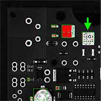
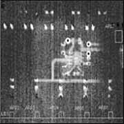
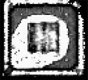
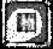
Residual image analysis and defect identification takes place after subtraction. The residual intensities are analysed by taking account of the context of original images. Firstly, a threshold operation is performed to highlight the residual pixels with high intensities. The optimal threshold is found from the histogram of the original image. Those pixels with high intensities are characterised as object pixels while others are characterised as background pixels.A grouping operation merges together separated pixels belonging to a common component - operations of medium filtering, corrosion, and void filling are applied so that isolated bright residual pixels can be eliminated and only thosebright spots corresponding to real missing components are retained. Subsequently, potential defects are identified when there are a group of bright pixels and, in addition, where their original image does not exhibit near-saturated intensities. Near-saturated intensities are most likely corresponding to surface shining. In Figure 2d line boxes are over-layed on the original target image by the AOI computer indicating suspected defects. The arrow indicates a false alarm due to shining of the soldering surface; this is highlighted for illustration purposes only. The AOI inspection module has been found to be particularly good at detecting missing components and misoriented components.
Fig.1. Finalised AOI inspection module prototype (with side panel removed)
|
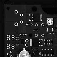
a) Golden reference image
|
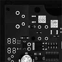
b) Inspected image
|
 |
 |
|
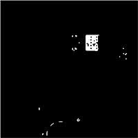
c) Final residual image after subtracting image (b)from (a)
|
d) Sentencing of potential defects
|
|
 |
|
Fig.2. AOI results for application of defect detection algorithms [Nicholson, Gao et al., 2006]
|
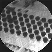
3.2 Digital Radiography (X-ray) inspection module
The development of the X-ray inspection module follows that of a basic 2D X-ray shadow imaging system (Bernard, 2003). The X-ray source is positioned at the bottom of a lead-lined chamber and a digital detector is positioned directly above. A PCB enters the chamber by means of edge conveyer belts and is positioned on a manipulator in-between the source and detector. Figure 3 shows the location of the conveyors and the X-ray source in the X-ray chamber. Out of view is the digital detector but this is recessed at the top of the chamber directly opposite to the X-ray source.
Fig.3. Main components inside X-ray chamber
The X-ray source is fully computer controlled. It is housed within a vacuum continuously pumped by a turbo-pump backed by a two-stage rotary-pump and monitored by a Penning gauge. It contains a microfocus electron gun with a magnetically focussed electron beam intercepting a 15µm air-cooled tungsten foil target behind a 0.5mm thick aluminium window. The X-rays are collimated at the source to a beam with a fan-angle of 14°. The cathode voltage is variable from 40 to 160 kV, and the maximum current is 500 µA, giving 20 watts target power at 40 kV.
The detection media system consists of a single field 6-inch aluminium window with an intensifier coupled via a large aperture lens to a digital camera. The camera produces images of 758 x 580 pixels and 12-bit depth with an adjustable frame rate of 25 fps and less, and is computer controlled. The nominal source to focus distance is 600mm, which allows magnifications of up to 1200 times depending on the sample position. Full details of the X-ray inspection module development have been reported. [Nicholson, Mitchard et al., 2006]
A manual X-ray system to recognise PCB defects was initially developed for static components to verify the basic operation of the system. A leaded glass window enables the operator to see the PCB. Afterwards the X-ray cabinet was modified to accept and interface a custom made PCB conveyor system. Particular attention had to be paid to X-ray safety, as the prototype was designed in such a way (to increase inspection throughput) that the conveyor entrance andexit was always open, giving the potential to expose X-rays outside of the prototype cabinet. X-rays naturally decay over distance according to the inverse square law. After simulation and empirical calculation, lead tunnels were developed with a certain length to keep radiation exposure to a recognised safe limit. In addition a collimator was developed to limit the radiation fan angle of the X-ray source.
A 5 axis manipulator system, housed in the X-ray chamber, was developed to enable the inspected PCB to be lifted from the conveyor, moved at different positions with respect to the X-ray source and detector, and then returned to the conveyor. Software algorithms were developed in order to detect poor Ball Grid Array (BGA) wetting and re-flow. A PCB gripper and scoop attached to the manipulator enabled the PCB to be held securely during inspection allowing for faster manipulator motion and the possibility to tilt the PCB at angles. Special consideration had to be made for the design of the gripper and scoop. Carbon fibre material was used for the scoop which is penetrable by X-rays, and is thus not visible in the X-ray images.
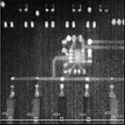
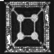
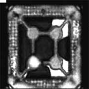
Figure 4 shows typical X-ray images obtained for a 256 ball BGA with a separation distance between PCB and X-ray source of 80mm. Figure 4a corresponds to a good component. The circular uniformity of balls, each relatively equal in area, is a good indication of complete and proper reflow of all the connections associated with the BGA. [Empfasis, 2002] Figures 4b and 4c correspond to a bad component with ball bridging and poor reflow respectively. It is immediately obvious with the artificially introduced bridging defect that solder balls are shorted. This defect was created by adding solder paste after printing, then placing the component and soldering. The poor reflow defect was created by manual placement of the component after reflow and with poor soldering with hot air. The oblong like shape of the solder balls connection is attributable to the wetting force of the molten solder. If all solder ball connections are not completely molten for a sufficient length of time, some joints will attempt to self-centre while others do not. [Empfasis, 2002]
For each inspected PCB, a preprogrammed script manipulates the PCB so that a particular BGA is positioned 80mm above the X-ray source. Using the same defect detection algorithms as those deployed for AOI inspection the X-ray inspection module is automatically able to sentence components as bad if their target image differs more than a predetermined percentage with respect to the golden reference image.
|
a) Golden reference image
|
b) Artificially introduced bridging defect
|
c) Artificially introduced poor reflow
|
 |
 |
 |
|
Fig.4. X-ray images for three different BGAs (70kV, 40.0uA)
|
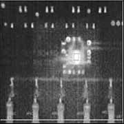
Tilting the PCB allows for angled X-ray images of BGAs which can be more revealing for certain defects such as poor BGA wetting. Poor BGA ball wetting is where there is poor contact of the ball to the solder and can be observed as balls that are not completely flat with the PCB pad (see Figure 5a). It is not possible to easily see this effect when viewing by X-ray directly above the BGA. This type of defect was especially prevalent when PCB manufacturers first switched from lead to lead free soldering processes, and often occurs when the lead free solder process is not optimised.
Algorithms, based on completely different techniques to those used for AOI sentencing, have been deployed to specifically test for poor BGA ball wetting. In order to classify the balls in the target image according to good or poor wetting, four main steps of image processing are carried out: pre-processing, segmentation (thresholding and separation of balls), shape feature extraction and classification. This has been previously reported. [Nicholson, Mitchard et al., 2006] Classification takes into account a number of features including the area, angle, height, width, curvature and roughness of the contour of each ball. Figure 5b shows a typical result of the poor wetted balls classification algorithm. The three lighter colour balls on the bottom row have been sentenced by the classification algorithm as poor wetted balls. Where balls in the target image cannot be distinguished as separate balls, after the application of thresholding and separation algorithms, these are ignored in the final sentencing.
|
a) Oblique view X-ray image of BGA
|
b) Classification of poor wetted balls
|
 |
 |
|
Fig.5. Application of poor BGA wetted balls classification
|
Ideally the PCB is tilted to allow for oblique angled X-ray images of BGAs. Tilting the PCB so that its orientation is from 40 to 60 degrees with respect to the X-ray source and detector can clearly reveal poor wetting in BGA balls. However, doing this on the current X-ray inspection prototype introduces a number of problems. Firstly, with the inclusion of the conveyor in the X-ray chamber, a compromise has to be made between tilt angle and magnification, since tilting the PCB necessitates increasing the distance between the PCB and X-ray source to avoid sample collision with either the source or the conveyor. An increased distance results in less magnification. Another problem is that, when viewing angled images, balls located behind other balls can be obscured and it is then not possible to reliably sentence a ball as a fail or pass. Finally, the manipulation required to angle and move the PCB, in order to image all the balls on the BGA, adds to the inspection time. This takes much longer compared to the subtraction algorithms which can sentence a good and bad BGA by imaging all the balls at the same time.
The BGA ball wetting classification algorithm still needs to be developed further and, in addition, a different technique for obtaining oblique angled X-ray images is necessary to make a more practical inspection system. However, for 2D X-ray imaging the system has proved to be very workable.
3.3 Thermography inspection module
Initial experiments were setup and conducted to establish the usefulness of thermography to detect various defects. Active thermography for detection of delamination of PCBs, and in the plastic packaging of Integrated Circuits (IC),was first investigated and has already been reported. [Avdelidis et al. 2006] In the active thermography setup, two 500W pulsed flash lamp illuminators were used to heat the PCB using a single flash. An Infra Red (IR) camera was used to record the images over a set period of time. However, it was concluded that it was easier to interpret and detect delamination type defects with other NDT techniques. In a second alternative approach of thermography, a passive thermography system was developed, but with the emphasis on short circuit detection. Employing a similar setup as for the AOI inspection module, including enclosure chamber and conveyor but replacing the vision camera with a 160 x 120 pixel IR camera and removing the light source, an automated system for detecting shorted components was developed. In passive thermography there is no application of an external heating source. However, in order to generate a heat signature there is a requirement to power the PCB. Similar to ICT, a mechanism was developed comprising a linear up/down actuator together with two attached spring loaded test pins. Power from a programmable power supply is fed to the test pins. When a PCB travelling along the conveyor is detected by anopto sensor, the conveyor is stopped and power applied to the PCB via the actuator.
Figure 6 shows inside the thermography prototype chamber just after the PCB has arrived. The IR camera is located in a fixed position above the area of interest on the PCB. The linear up/down actuator and spring loaded test pins are positioned above test pads located on the PCB ready to make contact.
Fig.6. Inside the thermography prototype chamber after the PCB has arrived
Once the PCB is powered, any short circuit will exhibit a thermal radiation signature that is different from its surroundings. Therefore, PCB circuit faults can be pin-pointed by the identification of 'hot spots' within the circuit.Sometimes it may even be possible to identify the component at fault itself, for an example an aluminium electrolytic capacitor installed with reversed polarity can generate excessive heat.
Similar to in-circuit tests, some planning ahead at the design stage of the PCB must take place to make the passive thermography inspection a success. In order to exercise the thermography inspection module, the 100 test PCBs thatwere manufactured for prototype testing included an active area containing a working circuit, together with test pads, to facilitate contact with the test pins. Various short circuited loads were introduced on each PCB, and applied across an active output of an IC via a combination of though-hole and surface mounted resistors.
Since passive thermography needs to apply power, and has the potential to be PCB and component destructive, a balance has to be made between applied voltages and powered board time duration. To minimise introduction of resulting component failure a lower 'power on' voltage should be selected but this is at the expense of requiring a longer 'power on' duration. Software was developed that enable Regions Of Interest (ROI) areas to be setup at different positions on the thermal signature. For each target PCB the ROI values were compared with predefined user thresholds to determine whether a PCB was defective.
Figure 7 shows typical thermal signatures for three inspected PCBs. When viewed in colour it is immediately apparent which components are exhibiting more heat dissipation as a result of an introduced short. In Figure 7 the lighter the colour the hotter the component. As more shorts are introduced the temperature of the IC can be seen to rise accordingly. The IR camera was able to detect changes in temperature to +/- 0.2°C. When all resistors were short circuited, and with a 5V power supply, the IC exhibited a temperature rise of 2.2°C in a period of just 10 seconds.
One caveat with thermography, and which is evident from the results, is that different materials exhibit different emissivity characteristics, i.e. the ratio of emissive power of a body compared to that of a perfect emitter (black body), having the same area and same temperature, differs according to material surface. From observation of the images in Figure 7 it can be seen that various tracks and pads appear to be hotter than the other components because the represented colour corresponds to the high end of the temperature scale. This is a false assumption as it is the high light reflectivity of some of these areas giving rise to different emissivity conditions. Emissivity correction values could be factored in the software when defining the ROIs, but this was not implemented in the prototype system. Instead when deciding where to put the ROIs the operator should be aware of the emissivity issues, i.e. choose a matt dull surface area of a component rather than a shiny surface for an ROI.
|
a) Passed PCB - no shorted resistors
|
b) Failed PCB - three shorted resistor
|
c) Failed PCB - all resistors shorted resistors
|
 |
 |
 |
|
Fig.7. Typical passive thermography results
|
A simple analogue circuit was used in the experiments, but the system could also be used for inspection of digital and microcomputer electronics to detect more subtle type defects. Preliminary experiments have shown it is possible to get different thermal images when a real digital circuit was in standby, initialised, and in 'power on' modes.
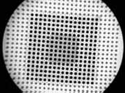
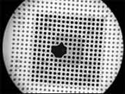
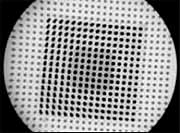
3.4 SAM Inspection module
In SAM inspection an ultrasonic probe is scanned above each component of interest. Water is used to provide the medium whereby ultrasonic waves can be transmitted from the probe into the component under inspection. Claims have been made that commercially available SAMs can be modified easily for in-line inspection. The solution is to mount samples in trays which are moved into the acoustic microscope by a robot. [Fassbender et al 2003] However, unlike such systems and reported here for the first time, it is only the prototype SAM developed for this project that can be claimed to be truly in-line. In-line operation is facilitated by the deployment of a water irrigation nozzle that enables the conveyor to pass easily under the water medium, but at the same time ensures that the PCB does not have to be submerged in a water bath as is the case for conventional SAMs. Another advantage is that this method also minimizes the chance of getting water trapped between a component and the PCB. Figure 8 shows ultrasonic scanning of a PCB using the irrigated water probe.
Fig.8. Scanning using irrigated water nozzle and 25MHz ultrasonic transducer
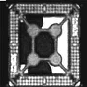
Initially, experiments were conducted with a conventional ultrasonic probe submerged in the water bath to establish optimal ultrasonic transducer inspection frequencies, together with experiments testing different scan steps for determining the minimum image acquisition time with the minimal acceptable image quality. Later experiments were repeated in conjunction with the irrigated water nozzle and image results were found to be near identical to those of the standard probe. Figure 9 shows results of different scan resolutions using a 25MHz ultrasonic probe in conjunction with the irrigated water nozzle. The component inspected is a BGA, and displays a typical delamination 'popcorn' defect. As can be seen from
Figure 9, the popcorn defect is still discernible at a step resolution of 0.5 mm. At this resolution, inspection throughput capability is at a maximum.
|
a) Resolution 0.15mm, Scan time = 25 s
|
b) Resolution 0.3mm, Scan time = 9 s
|
c) Resolution 0.5mm, Scan time = 6 s
|
 |
 |
 |
| Fig.9. Effect of reducing scan resolution on image detail |
|
a) QFP component - Golden reference
|
b) Bad QFP - Heat stressed from bottom side
|
c) Bad QFP - Heat stressed from top side
|
 |
 |
 |
|
Fig.10. Ultrasonic scans of a QFP IC
|
3.5 Systems Integration
Initially all the inspection module prototypes were developed and tested separately. Specifications were agreed between the developing partners from the outset of the project, and a standard industry interface, referred to as SMEMA [IPC, 2007] was adopted for each prototype. This facilitated the interfacing of the partner's equipment at a mechanical, electrical, and software communications level. At a mechanical level a common conveyor design was developed and incorporated a standard adjustable conveyor height, a fixed front rail, and adjustable rear rail able to accommodate PCB sizes of up to 200mm and a PCB edge clearance of no more than 5mm of clear board space at the side edges. At the electrical level a common control circuit was designed and developed to ensure compatibility between the prototypes. The adoption of the SMEMA standard means that, not only can the prototypes operate with each other, they can be immediately incorporated into most PCB surface mount manufacturing lines with little modification.
Each inspection module in the system is designed to operate in pull configuration for easy integration with another inspection module or other equipment on standard electronics manufacturing lines. Through utilisation of two signals' Machine Ready' and 'Board Available' transport of a PCB from one inspection module to another does not take place until called by the next downstream node. This eliminates the need for a separate cell controller for each node on the production line. [Burda, 1999]
Each inspection module has been designed so that a pass or failed component is indicated by an alarm, an on screen flag, and an entry saved to a results file local to each prototype. In addition each inspection prototype PC has the capability to be networked via 10/100 Ethernet, thus allowing a remote operator to interrogate all the prototype results files for statistical analysis from a single PC connected to the network.
Each module is controlled by a host PC. A common Input/Output (I/O) board was developed by TWI to facilitate a standardised electrical interfacing scheme for each inspection module. The I/O board accepts signals to/from the PCeither via USB, RS232 or PCI bus. The I/O module provides the signals for machine-to-machine communication and control of the conveyors. Figure 11 shows an overview of the final prototype indicating the signals used in the system. Figure 12 shows the inspection system as it has been setup in the laboratory.
Fig.11. Prototype System Overview combining the four inspection modules
Fig.12. The MICROSCAN Prototype PCB In-line inspection system
4 Discussion
Table 2 shows the approximate inspection throughput of each of the inspection techniques that have been combined to form the final Microscan prototype. For a PCB with component configurations as listed in Table 2 i.e. 30 SMT resistors, 1 BGA and 1 QFP the total inspection time is approximately 1.5 minutes per PCB. The throughput is very much dependent on the component type, PCB configuration and number of components. For some manufacturers the throughput of the final prototype could be an issue. In its current embodiment the prototype is more suited to high return PCB types such as those used in the medical and aerospace industries, rather than in high volume applications.
The X-ray inspection system and the SAM are the slowest of the inspection systems. As an example for a particular trial, a single 180 ball BGA was inspected and sentenced in around 40 seconds. For each inspection the board was lifted up, moved so that a component was in view and then returned back onto the conveyor. Having to orient the PCB to image more than one component, or change the board angle to image BGA poor ball wetting would take considerably longer.
Table 2 Inspection throughput of the final prototype
| | Inspection Module |
|---|
| AOI | X-ray | Thermography | SAM |
|---|
| Inspection Throughput |
30 SMT resistors/0.5 secs |
40 secs/BGA component |
14 secs/PCB |
13 secs/QFP component |
| Inspection area |
120mm2 |
180 ball BGA (15mm2 ) |
100mm2 |
QFP component (28mm2 ) |
| Type of defect |
Missing, flipped, misoriented component |
Missing balls, bridged balls, tilted BGA, poor reflow |
Short circuit |
Delamination/'popcorn' |
Table 1 lists the defects that were deemed as most important to detect. Although the list was a wish list, 14 out of the 25 defects are reliably detectable with the Microscan prototype. A number of defects (defect numbers 10,13, 14, 16, 17) not currently detectable are attributable to the AOI inspection module. This is because early on in the project a decision was made to keep the AOI system hardware simple and concentrate rather on the AOI algorithm development. There are two main limitations to the AOI setup. The fixed position high resolution camera has the advantage that image capture is instantaneous, however the bigger the area to be inspected on the PCB the bigger the distance the camera must be raised from the PCB in order to include all the ROIs in the field of view. This has the disadvantage that, for a given ROI, the resolution is degraded the higher the camera position from the PCB. Another disadvantage compared to commercially available AOI systems is that only a single light source is used. Therefore very small visual differences such as a 'lifted lead' or subtle changes in solder colour are not detected. An improvement to both AOI and thermography inspection modules would be the deployment of a flying camera.
5 Conclusion
An in-line inspection system comprising four different inspection techniques has been developed and a proof in principle has been demonstrated. The adoption of the SMEMA standard means that not only can the prototypes operate with each other, but they can be immediately incorporated into most PCB surface mount manufacturing lines with little modification.
Through the course of the development some new techniques have been introduced and applied to PCB inspection, including a water irrigation probe for SAM inspection and new algorithms for detecting BGA wetting. Further work is required in order to refine throughput and commercialise the system.
Acknowledgements
The results from this work are part of the CRAFT programme: Development of comprehensive in-line quality control system for printed circuit board assemblies, Acronym MICROSCAN, COOP-CT-2003-508613. MICROSCAN is a collaboration between the following organisations: TWI Ltd, X-TEK Systems Ltd, Lot Oriel GmbH, Machine Vision Products Inc, Microtel Technologie Elettroniche SpA, Beta Electronics Ltd, Ultrasonic Sciences Ltd, Goodrich Control Systems Ltd,Fraunhofer-Gesellschaft zur Foerderung der Angewandten Forschung E.V. and Kaunus University of Technology. The project is co-coordinated and managed by TWI Ltd and is partly funded by the EC.
References
- Avdelidis, N.P., Nicholson, P.I. and Wallace, P. (2006), 'Pulsed thermography in the investigation of PCBs for defect detection & analysis', Paper presented at 8th International Conference on Quantitative InfraRed Thermography, Padova, Italy, 28-30 June.
- Burda, R. (1999), 'Controlling Material Flow and WIP. on Existing Semiconductor Assembly. Equipment', Paper presented at SEMI TAP - Automation and. Integration Conference, 22-23 February.
- Empfasis (2002), 'X-ray inspection techniques for ball grid array and flip chip packages', A publication of the National Electronics Manufacturing Center of Excellence, available at www.empf.org/empfasis/feb02/xray02.htm, February.
- Fassbender, S.U. and Kraemer, K. (2003) 'Acoustic microscopy: a powerful tool to inspect microstructures of electronic devices', Proceedings of the SPIE, Testing, Reliability, and Application of Micro- and Nano-Material Systems. Vol. 5045, pp. 112-121.
- IPC (2007),'IPC-SMEMA-9851 Mechanical Equipment Interface Standard', available at www.ipc.org/html/IPC-SMEMA-9851.pdf, February.
- Mazeika, L., Kazys, R., Tumsys, O., and Gartside, C. (2007), 'Improvement of performance of scanning acoustic microscope for online inspection of electronic components', Proceedings of 4th International Conference Emerging Technologies in Non-Destructive Testing (ETNDT 4), Stuttgart, Germany, 2-4 April.
- Nicholson, P.I., Gao, J., Wallace, P., and Tomlinson, N. (2006),'Development of an automated optical imaging system for non destructive testing of PCBs', Proceedings of BINDT 2006 - The 45th Annual British Conference on Non-Destructive Testing, Stratford-upon-Avon, UK, 11-14 September.
- Nicholson, P.I., Mitchard, D., Forrest, C., Wallace, P., Bantel, T., Neumayer, D.A., and Haig, I. (2006), 'Development of an in-line X-ray system for automated inspection of defects of PCB assemblies containing BGAs', Proceedings of BINDT 2006 - The 45th Annual British Conference on Non-Destructive Testing, Stratford-upon-Avon, UK, 11-14 September.
- Nicholson, P.I. and Hardin, W. (2007), 'Spotlight on Market Opportunities: Multi technology system checks PCBs', Vision Systems Design, vol. 12, issue 8, August, pp. 49-50.
- Niermeyer, T. (2001), 'Where does AOI fit in PCB manufacturing?', Test and Measurement World, October.
- Oresjo, S. (1999), 'A new strategy for complex printed circuit board assemblies', Paper presented at Nepcon '99, California, USA, available at www.home.agilent.com/upload/cmc_upload/All/Nepcon99.pdf.
- Tlale, N.S., Bright, G., Potgieter, J. and Xu, P. (2002), 'Mechatronic modular design of an apparatus for PC board inspection', Proceedings for 2002 Australasian Conference on robotics and Automation, Auckland, 27-29 November.
- Verma, A., Ogden M. and Kokoska, J. (2000), 'Complementary test strategies on high-complexity boards', Circuits Assembly, CMP Media Inc, August.
- Veeser, S., Dunn, M.J. and Yang, G.Z. (2001), 'Multiresolution image registration for two-dimensional gel electrophoresis', Proteomics, Vol.1(7), July, pp. 856-870.
- Wen-Yen, W., Mao-Jiun, J.W. and Chih-Ming, L. (1996), 'Automated inspection of printed circuit boards through machine vision', Computers in industry, Vol. 28, Issue 2, May, pp. 103-111.
- Bernard, D., (2003), 'Selection Criteria for X-ray Inspection Systems for BGA and CSP Solder Joint Analysis', Paper presented at Nepcon, Shanghai/EMT China 2003, 8-11 April.
Further reading
www.microscan.eu.com
About the authors
P I Nicholson has over 15 years experience in microelectronics, sensor and software development. He holds a PhD inapplied magnetism and non destructive testing. He currently works as principal project scientist at TWI Technology Centre (Wales). His current research topics deal with non destructive testing methods for PCB inspection, systemsintegration and automating NDT inspection. Technical management of collaborative research projects is also an important activity, including the EU part funded research project titled 'MICROSCAN' leading to this publication. P INicholson is the corresponding author and can be contacted at
ian.nicholson@twi.co.ukP Wallace is section manager of 'The NDT Validation Centre' based in the Wales regional office of the TWI TechnologyCentre. With a background in electronics, materials science and applied chemistry, he also has 25 years experience as an NDT and manufacturing professional, primarily servicing the aerospace industry. He has a thorough practicalknowledge of a variety of NDT inspection techniques including radiography, eddy current, manual/automated penetrant inspection together with specialist knowledge of immersion Ultrasonic testing including Scanning AcousticMicroscopy.